Tour of Correlator Lab, 23 September 2011
Subject
Description
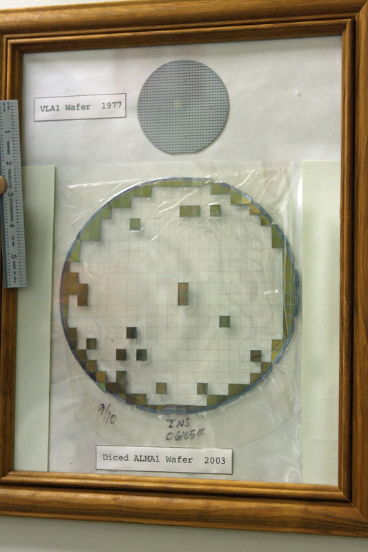
Framed display just outside the NTC Correlator Lab. It contains two wafers. A wafer is a thin, round piece of silicon with an array of integrated circuits fabricated on it. Each square is an integrated circuit. The wafer on the top contains integrated circuits called "VLA1" from the VLA correlator, fabricated in 1977. The wafer on the bottom contains integrated circuits called ALMA1 from the ALMA correlator, fabricated in 2003. The blank spaces in the bottom wafer are from chips that tested good and were packaged for installation on circuit board. Part of what the display shows is the difference in size of the physical wafers. In the 26 years between the fabrication of the two wafers, the technology had progressed to the point where much larger wafers could be fabricated. What you don't see in the comparison is the size of the features on the two wafers. Not only is the ALMA1 chip bigger, it also contains much smaller features.
Creator
Records of the NRAO
Type
Still Image
Identifier
2011Sep9CorrLab01.JPG
Original Format of Digital Item
Digital photograph
Location
Start Date
2011-09-23
Photographer
Photo Credit
NRAO/AUI/NSF
Notes
In September 2011, people from NRAO, Université de Bordeaux, and ALMA-Chile who had worked to design and build the ALMA correlator gathered to celebrate the correlator's completion.
Series
Photographs Series
Unit
MMA/ALMA Unit
Subunit
Charlottesville Correlator Lab Subunit
Collection
Citation
Records of the NRAO, “Tour of Correlator Lab, 23 September 2011,” NRAO/AUI Archives, accessed June 13, 2025, https://www.nrao.edu/archives/items/show/36845.

